Researchers have succeeded in upscaling high-quality graphene devices to the 100-micron scale and beyond. By perfecting CVD graphene production, transfer and patterning processes, scientists from the University of Hamburg and Graphenea manage to observe the quantum Hall effect in devices longer than 100 micrometers, with electronic properties on par with micromechanically exfoliated devices.
The work by Timothy Lyon and co-authors, published in Applied Physics Letters, started from graphene grown by chemical vapor deposition (CVD) on a copper substrate. CVD is the most successful technique for producing large-area high-quality graphene for high-tech applications. However, graphene on metal is not useful for applications in electronics, thus the material is usually transferred onto another substrate before use. The transfer process has proven to be a tough nut to crack, in many cases leading to cracks, defects, and chemical impurities that reduce the quality of the graphene.
In this most recent advance, researchers optimized every step of the transfer and patterning processes, resulting in large-area graphene of unprecedented quality. Transfer from copper was performed in eight consecutive steps, with three more steps needed to produce electrical contacts. Although the copper is removed with a standard etching solution, the bottom side of the graphene is cleaned with two reactive chemical etching steps to remove organic and inorganic contaminants. Also at other steps of the process, such as polymer removal, standard chemicals are replaced by carefully chosen ones in order to avoid graphene damage.

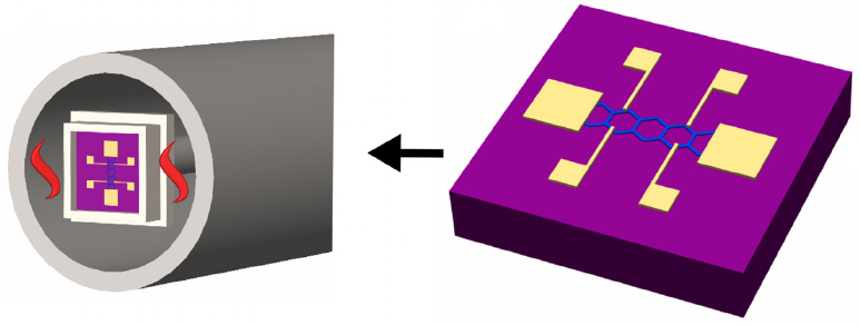
Figure: Graphene devices and measurement.
The optimized processing results in tear-free graphene on the desired Si/SiO2 substrate. Further processing is done to implement metallic contacts for electrical measurements. The electrical performance of the devices is measured in vacuum and at low temperature, revealing multiple quantum Hall levels. The quantum Hall effect on large scales opens the way to use graphene for universal electrical resistance standard measurements, hopefully leading to more precise measures of electron charge and the Planck constant.
The graphene devices have their charge neutrality point near zero gate voltage, which indicates very high material purity. Perhaps most importantly, the measured carrier mobility is as high as 3760 cm2/(Vs), which unambiguously shows that CVD graphene is an excellent candidate for electronic applications. Upscaling high-quality graphene device production beyond 100 microns is essential for commercial production. The authors of the research envisage such devices to find uses in THz-emitters, thermo-power couplers, and possibly flexible thin-film sensors.
via Graphenea
