There are advances being made almost daily in the disciplines required to make space and its contents accessible. This blog brings together a lot of that info, as it is reported, tracking the small steps into space that will make it just another place we carry out normal human economic, leisure and living activities.
Wednesday, 27 June 2018
NASA Again Delays Launch of Troubled Webb Telescope; Cost Estimate Rises to $9.7 Billion
The successor to the Hubble has had a series of mishaps during testing. An independent review board pushed back the launch for three years.
via New York Times
Trilobites: Oumuamua Is a Comet, Really.
First it was an alien comet, then maybe a spaceship, then an asteroid, now it’s a comet from way, way beyond.
via New York Times
Interstellar asteroid is really a comet
An object from another star system that made a brief appearance in our skies guised as an asteroid turns out to be a tiny interstellar comet.
via ESA Space Science
http://www.esa.int/Our_Activities/Space_Science/Interstellar_asteroid_is_really_a_comet
Complex organics bubble from the depths of ocean-world Enceladus
Data from the international Cassini spacecraft have revealed complex organic molecules originating from Saturn’s icy moon Enceladus, strengthening the idea that this ocean-world hosts conditions suitable for life.
via ESA Space Science
http://www.esa.int/Our_Activities/Space_Science/Cassini-Huygens/Complex_organics_bubble_from_the_depths_of_ocean-world_Enceladus
Graphene field-effect transistor (GFET) photodetectors
A surprising application of graphene is its use in photodetectors. Light detection capabilities of graphene are inherently limited because a single sheet of the material absorbs only ~2.3% of light across the visible part of the spectrum. Such high transparency is desired for applications such as transparent conductors, however detecting light requires strong absorption. Nevertheless, the frequency-independent absorption of graphene coupled with extremely high carrier mobility peaked the interest of optics researchers, who found that interfacing graphene with strong light-absorbing materials can result in excellent practical photodetectors that surpass the capabilities of competing materials.
First attempts of improving the photoresponse of graphene were in the direction of integration in nanocavities, microcavities, and plasmonic resonators, nano-engineered devices that locally increase the intensity of light, so that more response is obtained from the same graphene. These approached yield high sensitivity, however they restrict the usable bandwidth, cancelling the broadband nature of graphene. Spectrally broader response was obtained from hybrid graphene-quantum dot detectors, which however sacrificed device speed. Finally, a balance was achieved by laying graphene over photonic waveguides, increasing responsivity to 0.1 A/W with 20 GHz operation. The same working principle was since integrated in wafer-scale production and pushed to 75 GHz.
A particularly interesting direction of research is the use of hybrid graphene-quantum dot photodetectors as broadband image sensors for CMOS cameras. These fab-compatible devices have very high responsivity, on the order of 107 A/W and operate in both the visible and short-wave infrared parts of the spectrum (300-2,000 nm). The response times are fast enough (0.1-1 ms) for use in infrared cameras. What is perhaps the most interesting about this device is that it is a CMOS integrated circuit, similar to those used for commercial image sensors in digital cameras, commonly used in smartphones. Thus exploiting the full broadband capability of graphene, such chips will enable applications in safety and security, night vision, smartphone cameras, automotive sensor systems, food and pharmaceutical inspection, and environmental monitoring beyond capabilities offered by state-of-the-art semiconductor chips.

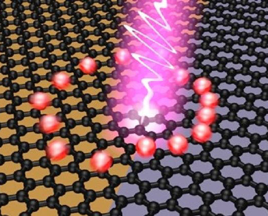
Illustration of photovoltage creation following light absorption in graphene (image copyright 2015 Achim Woessner)
Other approaches employ plasmon resonances to locally enhance intensity in graphene. Plasmons are light waves coupled to electron oscillations on the surface of a metal. Because plasmons are confined to a surface and because they propagate near the speed of light, they are considered by many as good candidates for on-chip optical information processing. Plasmon-enhanced photoresponse in graphene can have applications in nanoscale optoelectronic devices, where precise control of light behavior on dimensions smaller than half a wavelength is desired.
Other than for light detection, graphene can be used in light-emitting devices as well. An archetypal usage of graphene in such devices is as a transparent electrode. Transparent conductor applications are certainly an exciting application of graphene, because of its high transparency and extremely large carrier mobility. For example, graphene has been used as an electrode in organic light emitting diodes (OLEDs) which compose many of today’s screens and monitors. Another use, again enabled by graphene’s unusual electronic properties, is electrical control of light emission from molecules, with potential applications in optoelectronics.
Photodetection is one of many interesting uses of graphene. Some types of graphene-based photodetectors, for example the ones that utilize quantum dots or surface plasmons, can make use of graphene field effect transistors (GFETs). Researchers working in this field can now benefit from ready-made GFETs available from Graphenea, reducing the entry barriers and speeding up device development.
via Graphenea
Graphene forms electrically charged crinkles
Gently compressed stacks of graphene form sharp crinkles that carry an electric charge, which could be useful in nanoscale self-assembly and other applications.
via Science Daily
Postcards from Mars
The ExoMars orbiter sends a selection of images from around the Red Planet
via ESA Space Science
http://www.esa.int/Our_Activities/Space_Science/ExoMars/Highlights/Postcards_from_Mars